An interface of chiral electronic structures
Dirac Fermions, spin-polarization, and charge density waves

This week I’m joining Dr. Tobias Ritschel (TU Dresden, PDQM) for an ARPES experiment at the BESSY-II synchrotron in Berlin. The goal of the experiment is to grow a single sheet of TaSe2 (i.e. a selenium-tantalum-selenium sandwich) on top of a Bi2Se3 crystal and then test if it likes to form a charge density wave when cooled.
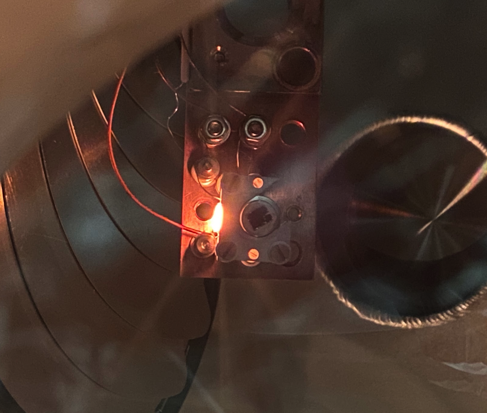
Bi2Se3 crystal ready for the experiment
In heavy elements like Tantalum, the motion and spin of electrons are strongly coupled. In the Se-Ta-Se sandwich, this means that the way in which the charge carriers move through the material depends on whether their spins point up or down. The plot thickens when this TaSe2 sheet lies on the surface of a Bi2Se3 crystal. This material is a three-dimensional topological insulator - it’s insulating in the bulk, but its electronic states are tied up in a way that they must form a knot on every surface. These surface states for channels in which the charge carriers behave like Dirac Fermions - move freely with an extraordinary, with extraordinary mobility. The Dirac Fermions don’t get into each other’s way, because, just as in the TaSe2 sheet, charge carriers of each spin channel stay in their lane. But what happens if you connect the two?

Lótus Bridge
Eight kilometers west of Macau Intl. Airport, civil engineers had to get creative to match transport conventions of opposite chirality. By growing TaSe2 on Bi2Se3, we might force Dirac fermions into a similar dilemma.
Together with collaborators from the MPI for Microstructure Physics and other institutes, Tobias has already been able to study the electronic structure of the TaSe2|Bi2Se3 system. They recently reported this in Polyakov et al., Nature Communications 13, 2472 (2022). The beautiful spin-resolved ARPES (angle-resolved photoemission spectroscopy) data and DFT (density functional theory) calculations in this paper shows that to satisfy the Pauli principle of quantum mechanics, the charge carriers above and below the interface choose opposite chiralities.
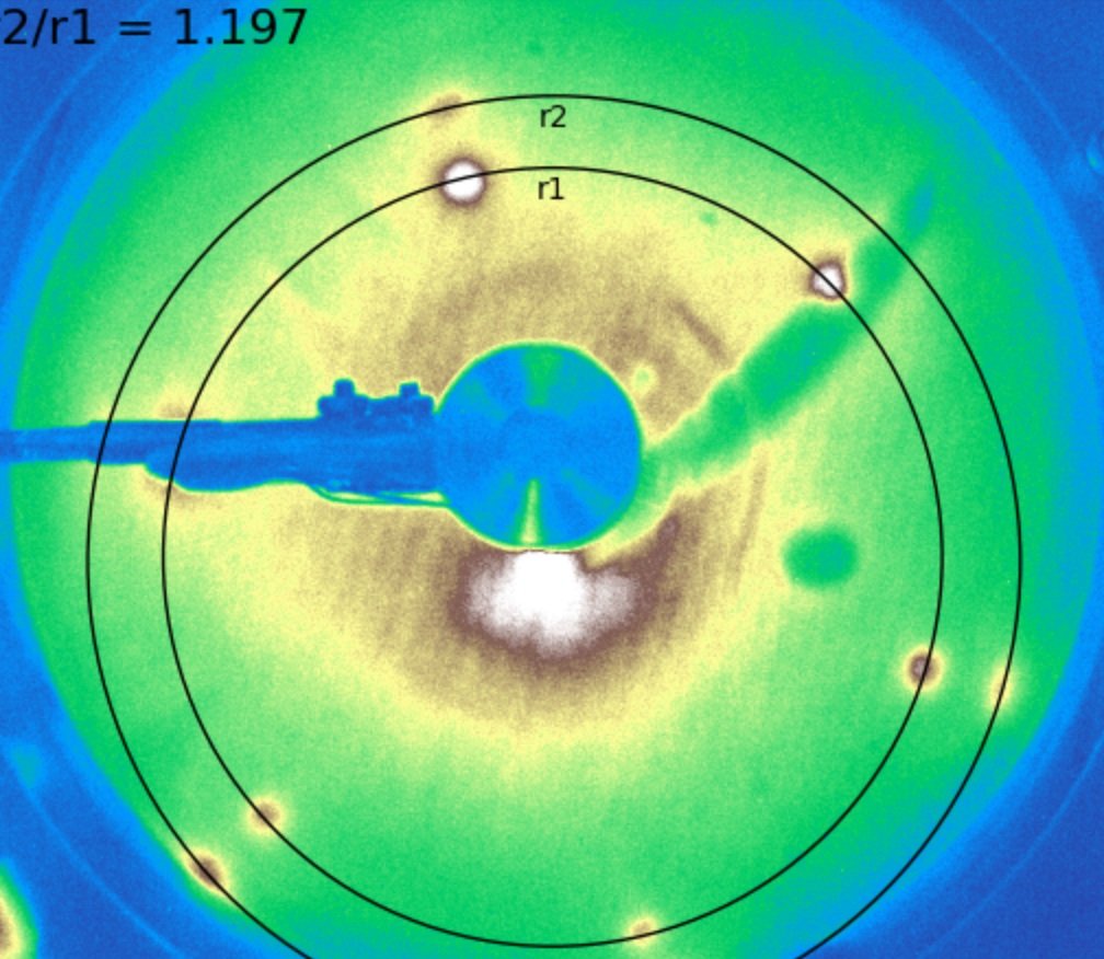
The reason why we want to revisit the Polyakov et al. study at BESSY-II/HZB is that here we can reach very low sample temperatures. In fact, the One-Cube instrument is the only sychrotron ARPES instrument that provides sample temperatures down to almost 1K. TaSe2 should also form a charge density wave at low temperatures. At least it does in the bulk, and also in TaSe2 films made by molecular beam epitaxy (see e.g. the ARPES study by Ryu et al. (2018)) or exfoliation (Raman study by Hajiyev et al.). This charge density wave would reconstruct the electronic states of the TaSe2 sandwich and create topologically protected conduction channels, similar to the Bi2Se3 substrate.

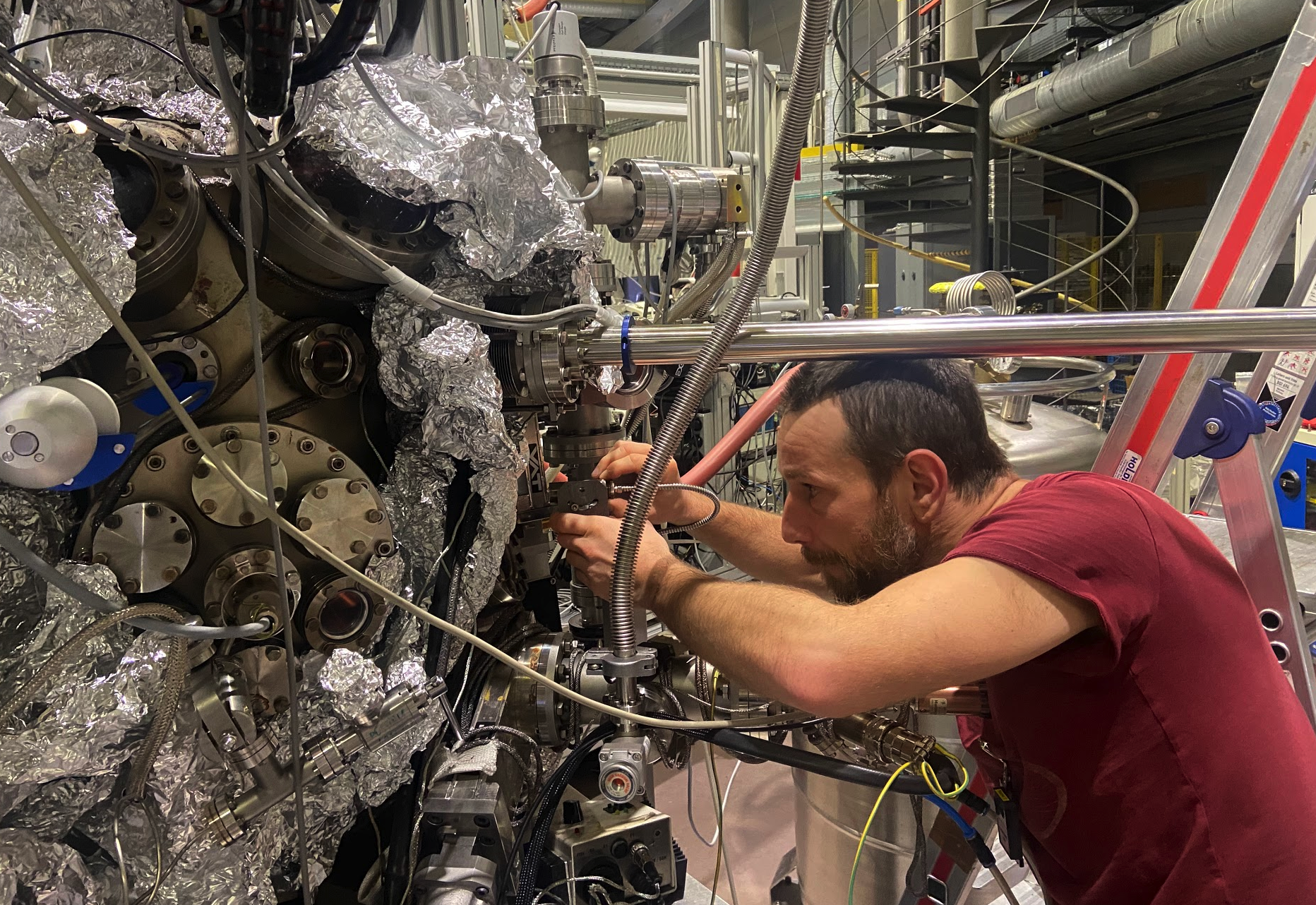
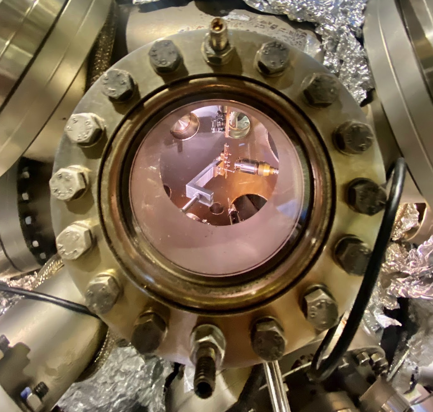
Tobias setting up the experiment at the ARPES instrument One-Cube at the BESSY-II synchrotron in Adlershof, Berlin (part of Helmholtz-Zentrum Berlin).
To create our Se-Ta-Se sandwich, we are actually using neither epitaxy, nor exfoliation, but a special trick: First we evaporated tantalum onto the Bi2Se3 crystal, which creates an amorphous (disordered) layer of atoms. When we heat it to ~500C for a few minutes, selenium creeps out of the substrates and assembles a neat TaSe2 layer.